Stage1

The first stage of the DSi's bootloader lives in ROM, on the CPU-TWL SoC die. It loads further encrypted+signed stages from the selected boot medium (usually NAND flash), starting with a plaintext offset table in the sector at offset 0x200. The code of the ROMs live at the upper 32k of the BIOS memory areas, i.e. at 0xffff8000 for the ARM9, and 0x00008000 for the ARM7.
The bootroms perform the following steps to load, verify and decrypt the second-stage bootloader:
- Perform some initialization, such as clearing and setting up the .data and .bss sections, setting up the MPU and an RSA heap (ARM9), and the AES hardware (ARM7).
- At this moment, main RAM (aka FCRAM aka DRAM) isn't initialized yet, and is unusable. It is only initialized at the very beginning of stage2.
- The ARM9 initializes its DTCM to reside at 0x02ff8000, an area normally backed by DRAM that also contains the exception vectors. DTCM is marked as no-execute, and the NWRAM area is marked as cacheable. ITCM is r/w/x.
- Read configuration bytes from NVRAM: the first 0x28 bytes and the single byte at 0x2ff are loaded.
- Decide on the boot medium:
- If the magic key combination "X+start+select+lid down" is held down and a game cartridge is inserted, booting from it is attempted (much like the 3DS boot ROMs). Note that the contents of the game cartridge must adhere to the regular stage2 header format, so booting from retail game cartridges won't work.
- If the most significant bit of the byte at 0x2ff of NVRAM is high, NAND will be used as a boot medium.
- As a fallback, the console will try to boot from NVRAM. (On retail consoles, this always fails as NVRAM does not contain any bootcode.)
- If one boot method fails, the bootroms will continue trying with the next one.
- 0x200 bytes at offset 0x200 from the boot medium are read. This contains the stage2 header. (For gamecart boots, the offset is 0 instead.)
- The RSA signature of the stage2 header is verified, and the first two SHA1 hashes (of the rest of the stage2 header, and the hash of the RSA message itself) are verified.
- On failure, goto 10.
- On success, the ARM9 instructs the ARM7 to load and decrypt the stage2 ARM7 binary from the boot medium. DMA is used from the boot medium to the AES hardware, but the output of the AES accelerator is simply read by software.
- Depending on the option bits in the stage2 header, this payload may be compressed.
- Uncompressed payloads are loaded into NWRAM on the ARM7 side, and then mapped to the ARM9 using the MBK registers.
- For compressed payloads, either the above can happen too, or the compressed data can first be sent to the ARM9 using the IPC FIFO, where the latter then performs the decompression.
- After the loading happens, the SHA1 hash is checked, but the result is not yet communicated.
- The above is repeated for the stage2 ARM9 binary.
- Only once both binaries have been checked will the ARM9 communicate the hash comparison result to the ARM7.
- On failure, both cores will lock up, and the ARM9 will display an error code on the top screen (see below).
- On success, both cores will:
- Deinitialize some hardware (partially clear RAM, deinitialize the MPU, etc.)
- Prepare keys for the next bootstage (some in the AES hardware, others copied to WRAM or ITCM)
- The ARM7 will lock out both boot ROMs from the system memory bus using the SCFG registers. The ARM9 waits for this lockout to happen.
- Both cores, now synchronized using the lockout, will now jump to stage2 code. (Current stage2 binaries will immediately re-synchronize the cores, however.)
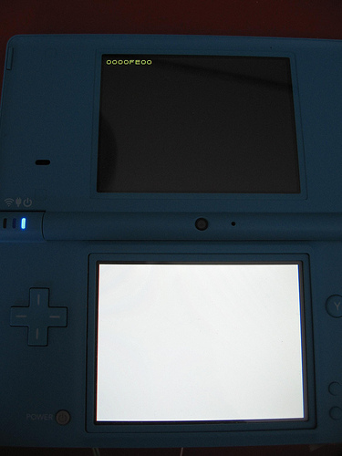
Error codes are supposed to be interpreted as a 32-bit unsigned little-endian integer, the least significant byte describing the status of the NAND boot attempt, the next of the NVRAM boot attempt, and the third one describes the game cartridge boot attempt. The most significant byte is always 0.
The individual bytes carry the following meaning:
- 00: The boot method has not been attempted, or failed during physical initialization (eg. NAND clk shorted, or no cartridge was inserted when attempting a game cartridge boot).
- FE: stage2 header verification failed.
- FD: stage2 ARM7 binary verification failed.
- FC: stage2 ARM9 binary verification failed.
The boot ROM does not use any other error codes.
In practice, the error codes carry the following meanings:
| Error Code | Description |
|---|---|
| 00FxFExx | Failed to run ntrboot exploit. |
| 0000FE00 | Error communicating with NAND chip (it's missing, CLK is shorted, etc.), or the most significant bit of the byte at 0x2ff of NVRAM has been cleared. (If you have a modchip installed, it could also mean the modchip exploit failed.) |
| 0000FEFC | Integrity error in ARM9 info block of Stage 2 (address at 0x220) |
| 0000FEFD | Integrity error in ARM7 info block of Stage 2 (address at 0x230) |
| 0000FEFE | Integrity error in the stage2 header (or error in NVRAM header: first 40 bytes must have a specific value). |