Hardware: Difference between revisions
Jump to navigation
Jump to search
FloralDelux (talk | contribs) |
|||
| (53 intermediate revisions by 24 users not shown) | |||
| Line 1: | Line 1: | ||
== Specifications == | |||
* [[Cameras|Two Aptina MT9V113 0.3 Megapixel VGA Cameras]] | |||
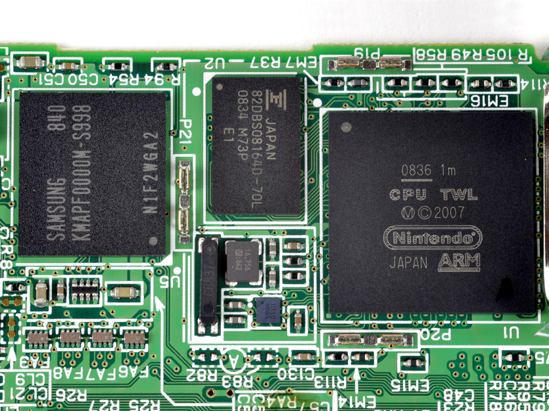
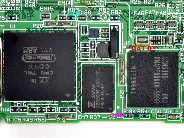
* 240MB(+16MB probably reserved for wear leveling purposes (e.g. replacing bad blocks)) eMMC NAND - Samsung KMAPF0000M-S998 Movi[[NAND]] or Samsung KLM5617EFW-B301 [[NAND]] | |||
* 16MB RAM - NEC uPD 46128512AF1 DDR SRAM or a Fujitsu 128-Mbit FCRAM 82DBS08164D-70L (datasheet: http://edevice.fujitsu.com/fj/DATASHEET/e-ds/e511454.pdf mirror:[[Media:E511454.pdf]] | |||
* (2) 256 x 192 3.25 Inch Displays, one of which has a resistive touch screen | |||
* Backwards compatible with Nintendo DS games, but not GBA games due to the lack of a gameboy cartridge port. | |||
* Integrated ARM946E-S core clocked at 133 MHz in real mode and downclocked to 66 MHz for compatibility mode. ARM7TDMI at 33 MHz. Additional CEVA XpertTeak DSP core, also running at 133 MHz | |||
* PAIC3000D Touchscreen and sound controller - possibly a TI codec: TSC2117 | |||
* Mitsumi (MM3317A) or TI 72071B0 or NEC UPD68878Y04 - Power management controller. (The charger circuit itself is fully analog, and closer to the charging port.) | |||
* SD/SDHC Card slot | |||
* [[WiFi_Module]] with integrated 128KB SPI Flash for [[NVRAM]], WiFi settings | |||
* BPTWL - Microcontroller based on a NEC uPD78F0500 used as "Super I/O"/"Embedded controller", used for battery charge level monitoring, volume settings, power-on sequencing of various modules (SoC, Wifi, ...), basic troubleshooting of the power supplies. Controls the status LEDs in the hinge, and the camera LED (near the outer camera). | |||
== Hardware Revisions == | |||
=== DSi === | |||
* board C/TWL-CPU-01 (Original rev, all pictures below) | |||
* CPU: TWL. The latest date code picture I could find online was "0836 1m" as shown below, however other pictures with CPU covered show the NAND codes as late as 916, so... | |||
* Suspect this is the only board where WiFi chip is available in Hybrid games like CookingCoach | |||
* Wireless card DWM-W015 | |||
== | === DSi RevA === | ||
* | * board C/TWL-CPU-10 (Newer model, can someone provide a date or serial # range?) | ||
* | * CPU: TWL A. Mine is "0937 1k". My US Serial # is ~ TW43550???[8]. It was obtained around the holiday season of 2009. If yours is earlier, please update this. | ||
===== TWL-USA-1 ===== | |||
* | * It is unclear what the difference between the USA-1 and USA models is, might indicate the presence of the KLM5617EFW-B301 NAND chip | ||
* CPU: TWL A. Mine is "1034 7m". My US-1 Serial # is ~ TW45013???[9]. | |||
== | === DSi XL === | ||
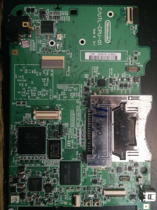
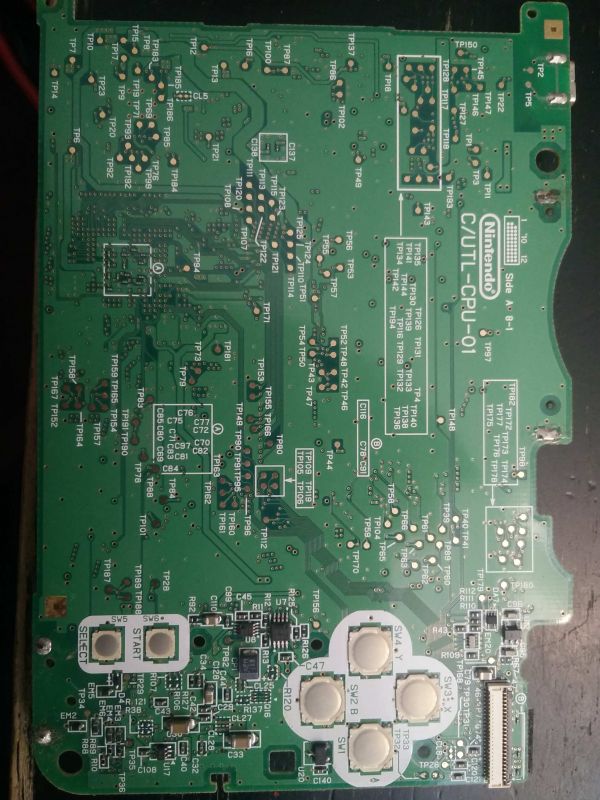
* board C/UTL-CPU-01 | |||
* CPU is TWL A | |||
* Wireless card DWM-W024 | |||
== Images == | |||
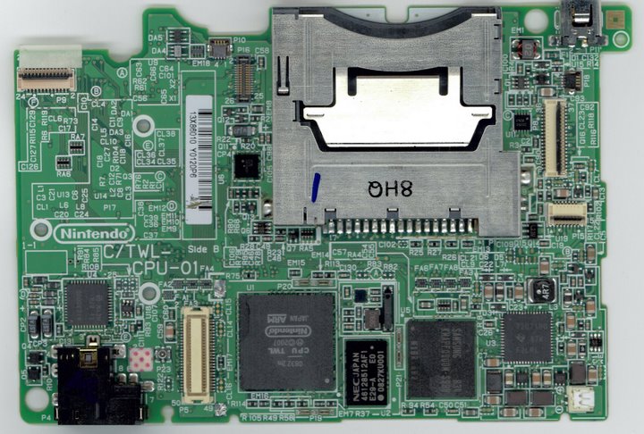
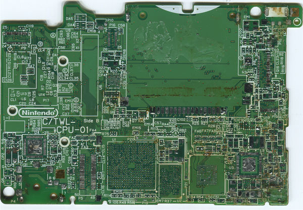
=== DSi Front === | |||
[[Image:Twl_front.jpg]] | |||
[[Image:Twl_front_traces.jpg|600px]] | |||
[[Image:TWL-CPU-10.png]] | |||
The socket to the left of the ARM processor is the wifi chip socket. | |||
TWL CPU pinout map: [[File:Twl_cpu_pinout.pdf]] (WIP) | |||
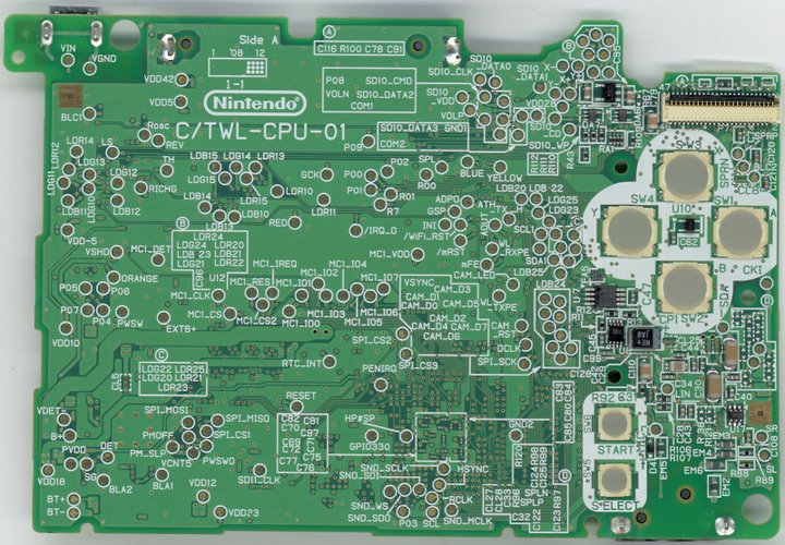
=== DSi Back === | |||
[[Image:Twl_back.jpg]] | |||
[[Image: | === CPU with New RAM === | ||
[[Image:CPUv2.jpg]] | |||
=== DSi XL Front === | |||
[[Image:Utl-cpu-01-sideb.jpg|600px]] | |||
=== DSi XL Back === | |||
[[Image:Utl-cpu-01-sidea.jpg|600px]] | |||
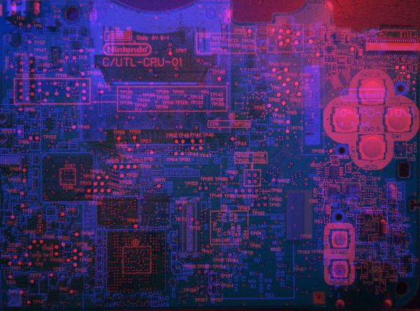
Testpoint list [[DSi XL testpoints|here]] | |||
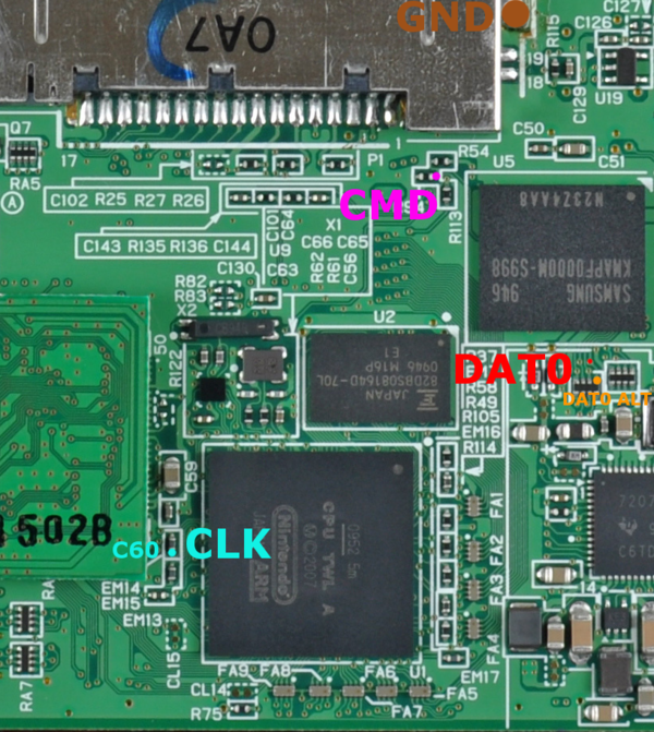
== NAND Pinout == | |||
[[Image:Dsi_nand.jpg|600px]] | |||
[[Image:Dsi_nanddat.png|600px]] | |||
=== DSi === | |||
[[Image:NAND_Compressed.jpg|600px]] | |||
=== DSi XL === | |||
[[Image:Side_B_Marked_Compressed.png|600px]] | |||
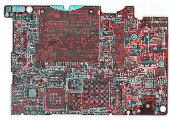
== PCB Overlay == | |||
=== DSi === | |||
[[Image:Nintendo DSi PCB Layered.jpg|600px]] | |||
=== DSi XL === | |||
[[Image:Utl-pcb-overlay.jpg|600px]] | |||
[[Image: | == Glamor Shot == | ||
[[Image:Nintendo-dsi-Glamor-Shot.jpg]] | |||
== References == | == References == | ||
* http://en.wikipedia.org/wiki/Nintendo_DSi | |||
* http://insidetronics.blogspot.com/2008/11/new-nintendo-dsi-teardown.html | |||
* http://techon.nikkeibp.co.jp/english/NEWS_EN/20081111/161077/ | |||
* http://games.gearlive.com/playfeed/article/q408-nintendo-dsi-announced-larger-screens-dual-cameras-dsi-shop-store/ | |||
* http://www.ifixit.com/Guide/First-Look/Nintendo-DSi/714/1 | |||
Latest revision as of 17:44, 4 October 2023
Specifications
- Two Aptina MT9V113 0.3 Megapixel VGA Cameras
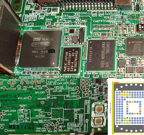
- 240MB(+16MB probably reserved for wear leveling purposes (e.g. replacing bad blocks)) eMMC NAND - Samsung KMAPF0000M-S998 MoviNAND or Samsung KLM5617EFW-B301 NAND
- 16MB RAM - NEC uPD 46128512AF1 DDR SRAM or a Fujitsu 128-Mbit FCRAM 82DBS08164D-70L (datasheet: http://edevice.fujitsu.com/fj/DATASHEET/e-ds/e511454.pdf mirror:Media:E511454.pdf
- (2) 256 x 192 3.25 Inch Displays, one of which has a resistive touch screen
- Backwards compatible with Nintendo DS games, but not GBA games due to the lack of a gameboy cartridge port.
- Integrated ARM946E-S core clocked at 133 MHz in real mode and downclocked to 66 MHz for compatibility mode. ARM7TDMI at 33 MHz. Additional CEVA XpertTeak DSP core, also running at 133 MHz
- PAIC3000D Touchscreen and sound controller - possibly a TI codec: TSC2117
- Mitsumi (MM3317A) or TI 72071B0 or NEC UPD68878Y04 - Power management controller. (The charger circuit itself is fully analog, and closer to the charging port.)
- SD/SDHC Card slot
- WiFi_Module with integrated 128KB SPI Flash for NVRAM, WiFi settings
- BPTWL - Microcontroller based on a NEC uPD78F0500 used as "Super I/O"/"Embedded controller", used for battery charge level monitoring, volume settings, power-on sequencing of various modules (SoC, Wifi, ...), basic troubleshooting of the power supplies. Controls the status LEDs in the hinge, and the camera LED (near the outer camera).
Hardware Revisions
DSi
- board C/TWL-CPU-01 (Original rev, all pictures below)
- CPU: TWL. The latest date code picture I could find online was "0836 1m" as shown below, however other pictures with CPU covered show the NAND codes as late as 916, so...
- Suspect this is the only board where WiFi chip is available in Hybrid games like CookingCoach
- Wireless card DWM-W015
DSi RevA
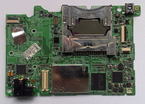
- board C/TWL-CPU-10 (Newer model, can someone provide a date or serial # range?)
- CPU: TWL A. Mine is "0937 1k". My US Serial # is ~ TW43550???[8]. It was obtained around the holiday season of 2009. If yours is earlier, please update this.
TWL-USA-1
- It is unclear what the difference between the USA-1 and USA models is, might indicate the presence of the KLM5617EFW-B301 NAND chip
- CPU: TWL A. Mine is "1034 7m". My US-1 Serial # is ~ TW45013???[9].
DSi XL
- board C/UTL-CPU-01
- CPU is TWL A
- Wireless card DWM-W024
Images
DSi Front
The socket to the left of the ARM processor is the wifi chip socket.
TWL CPU pinout map: File:Twl cpu pinout.pdf (WIP)
DSi Back
CPU with New RAM
DSi XL Front
DSi XL Back
Testpoint list here
NAND Pinout
DSi
DSi XL
PCB Overlay
DSi
DSi XL
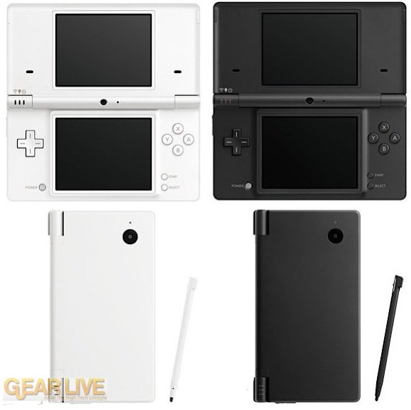
Glamor Shot
References
- http://en.wikipedia.org/wiki/Nintendo_DSi
- http://insidetronics.blogspot.com/2008/11/new-nintendo-dsi-teardown.html
- http://techon.nikkeibp.co.jp/english/NEWS_EN/20081111/161077/
- http://games.gearlive.com/playfeed/article/q408-nintendo-dsi-announced-larger-screens-dual-cameras-dsi-shop-store/
- http://www.ifixit.com/Guide/First-Look/Nintendo-DSi/714/1
