Hardware: Difference between revisions
Jump to navigation
Jump to search
mNo edit summary |
Updated Headers, added conventional pinouts for DSi and DSiXL |
||
| Line 1: | Line 1: | ||
= Specifications = | |||
*[[Cameras|Includes (2) 0.3 Megapixel VGA Cameras]] | *[[Cameras|Includes (2) 0.3 Megapixel VGA Cameras]] | ||
| Line 14: | Line 12: | ||
*[[WiFi_Module]] with integrated 128KB SPI Flash for [[NVRAM]], WiFi settings | *[[WiFi_Module]] with integrated 128KB SPI Flash for [[NVRAM]], WiFi settings | ||
= Hardware Revisions = | |||
== DSi == | |||
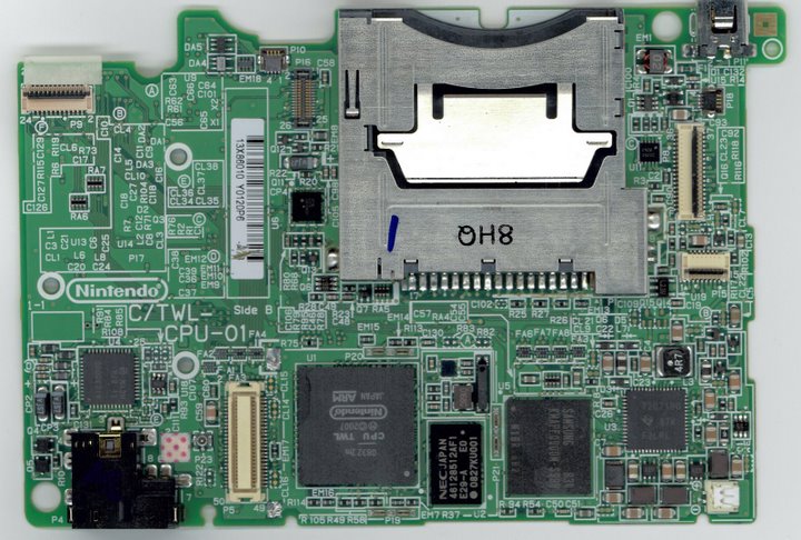
** board C/TWL-CPU-01 (Original rev, all pictures below) | ** board C/TWL-CPU-01 (Original rev, all pictures below) | ||
** CPU: TWL. The latest date code picture I could find online was "0836 1m" as shown below, however other pictures with CPU covered show the NAND codes as late as 916, so... | ** CPU: TWL. The latest date code picture I could find online was "0836 1m" as shown below, however other pictures with CPU covered show the NAND codes as late as 916, so... | ||
| Line 21: | Line 23: | ||
** Wireless card DWM-W015 | ** Wireless card DWM-W015 | ||
== DSi RevA == | |||
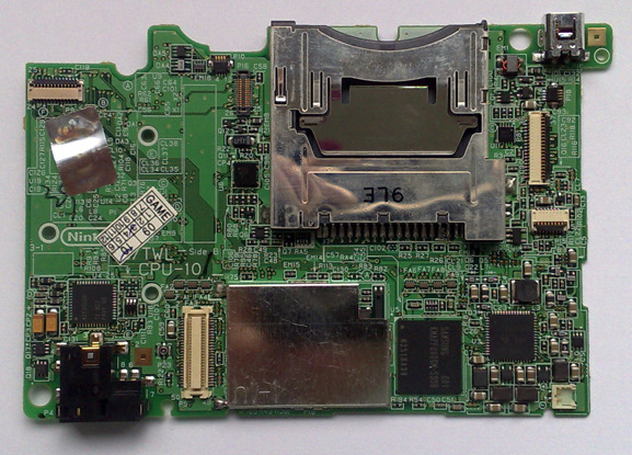
** board C/TWL-CPU-10 (Newer model, can someone provide a date or serial # range?) | ** board C/TWL-CPU-10 (Newer model, can someone provide a date or serial # range?) | ||
** CPU: TWL A. Mine is "0940 2m". My US Serial # is ~ TW71848???[5]. If yours is earlier, please update this. | ** CPU: TWL A. Mine is "0940 2m". My US Serial # is ~ TW71848???[5]. If yours is earlier, please update this. | ||
| Line 27: | Line 30: | ||
== DSi XL == | |||
** board C/UTL-CPU-01 | ** board C/UTL-CPU-01 | ||
** CPU is TWL A | ** CPU is TWL A | ||
** Wireless card DWM-W024 | ** Wireless card DWM-W024 | ||
= Images = | |||
== Front == | |||
[[Image:Twl_front.jpg]] | [[Image:Twl_front.jpg]] | ||
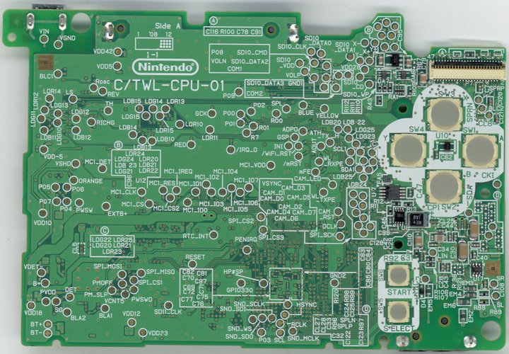
[[Image:Twl_front_traces.jpg|600px]] | [[Image:Twl_front_traces.jpg|600px]] | ||
| Line 43: | Line 48: | ||
TWL CPU pinout map: [[File:Twl_cpu_pinout.pdf]] (WIP) | TWL CPU pinout map: [[File:Twl_cpu_pinout.pdf]] (WIP) | ||
== Back == | |||
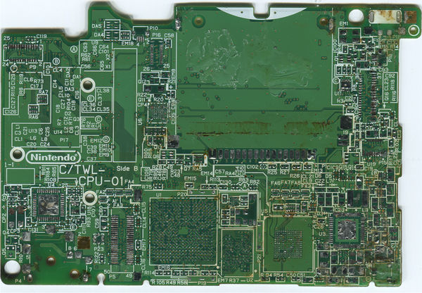
[[Image:Twl_back.jpg]] | [[Image:Twl_back.jpg]] | ||
== NAND Pinout == | |||
[[Image:Dsi_nand.jpg|600px]] | [[Image:Dsi_nand.jpg|600px]] | ||
[[Image:Dsi_nanddat.png|600px]] | [[Image:Dsi_nanddat.png|600px]] | ||
=== PCB | |||
== NAND Pinout With Conventional Markings == | |||
===DSi=== | |||
[[Image:NAND_Compressed.jpg|600px]] | |||
===DSi XL=== | |||
[[Image:Side_B_Marked_Compressed.png|600px]] | |||
== PCB Overlay == | |||
[[Image:Nintendo DSi PCB Layered.jpg|600px]] | [[Image:Nintendo DSi PCB Layered.jpg|600px]] | ||
== CPU with New RAM == | |||
[[Image:CPUv2.jpg]] | [[Image:CPUv2.jpg]] | ||
== Glamor Shot == | |||
[[Image:Nintendo-dsi-Glamor-Shot.jpg]] | [[Image:Nintendo-dsi-Glamor-Shot.jpg]] | ||
== References == | == References == | ||
# http://en.wikipedia.org/wiki/Nintendo_DSi | # http://en.wikipedia.org/wiki/Nintendo_DSi | ||
# http://insidetronics.blogspot.com/2008/11/new-nintendo-dsi-teardown.html | # http://insidetronics.blogspot.com/2008/11/new-nintendo-dsi-teardown.html | ||
Revision as of 23:11, 19 March 2016
Specifications
- Includes (2) 0.3 Megapixel VGA Cameras
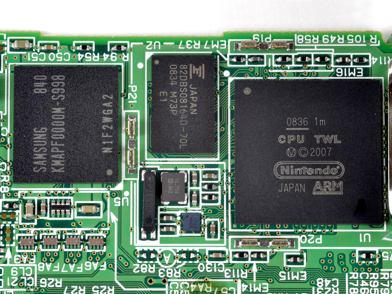
- 240MB(+16MB probably reserved for wear leveling purposes (e.g. replacing bad blocks)) Internal Flash Memory - Samsung kmapf0000m-S998 MOVI NAND - MMC Interface
- 16MB RAM - NEC uPD 46128512AF1 - DDR SRAM or a Fujitsu 128-Mbit FCRAM 82DBS08164D-70L (datasheet: http://edevice.fujitsu.com/fj/DATASHEET/e-ds/e511454.pdf mirror:Media:E511454.pdf
- (2) 256 x 192 3.25 Inch Displays, one of which has a resistive touch screen
- Backwards compatible with Nintendo DS games but not GBA games due to the lack of a gameboy cartridge port.
- Integrated ARM7/ARM9 cores clocked at 133mhz in real mode and downclocked to 66mhz for compatibility mode.
- PAIC3000D Sound Chip - possibly a TI codecs: AIC3 ????
- Mitsumi (MM3317A) or TI 72071B0 - Power supply and charger circuit ????
- SD/SDHC Card slot
- WiFi_Module with integrated 128KB SPI Flash for NVRAM, WiFi settings
Hardware Revisions
DSi
- board C/TWL-CPU-01 (Original rev, all pictures below)
- CPU: TWL. The latest date code picture I could find online was "0836 1m" as shown below, however other pictures with CPU covered show the NAND codes as late as 916, so...
- Suspect this is the only board where WiFi chip is available in Hybrid games like CookingCoach
- Wireless card DWM-W015
DSi RevA
- board C/TWL-CPU-10 (Newer model, can someone provide a date or serial # range?)
- CPU: TWL A. Mine is "0940 2m". My US Serial # is ~ TW71848???[5]. If yours is earlier, please update this.
DSi XL
- board C/UTL-CPU-01
- CPU is TWL A
- Wireless card DWM-W024
Images
Front
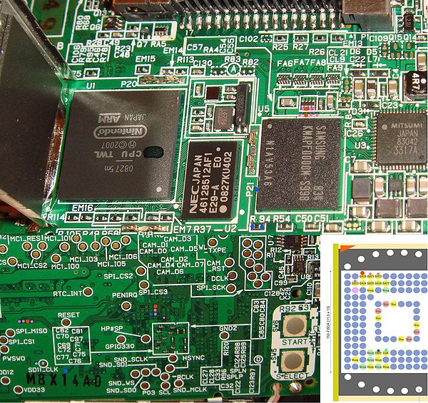
The socket to the left of the ARM processor is the wifi chip socket.
TWL CPU pinout map: File:Twl cpu pinout.pdf (WIP)
Back
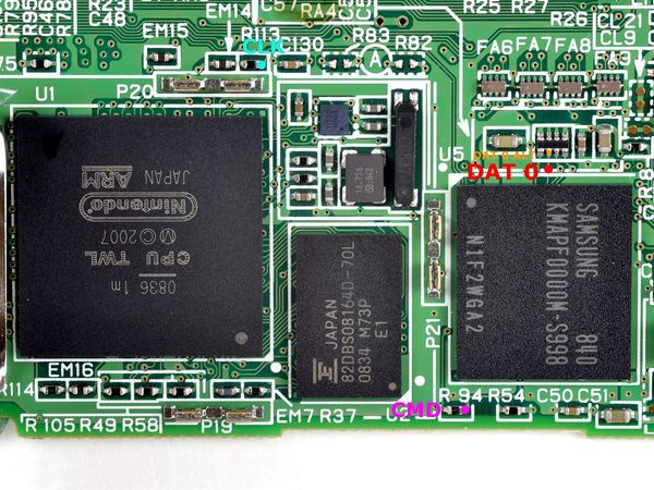
NAND Pinout
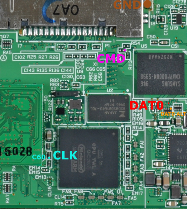
NAND Pinout With Conventional Markings
DSi
DSi XL
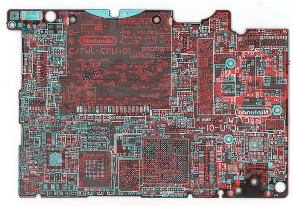
PCB Overlay
CPU with New RAM
Glamor Shot
References
- http://en.wikipedia.org/wiki/Nintendo_DSi
- http://insidetronics.blogspot.com/2008/11/new-nintendo-dsi-teardown.html
- http://techon.nikkeibp.co.jp/english/NEWS_EN/20081111/161077/
- http://games.gearlive.com/playfeed/article/q408-nintendo-dsi-announced-larger-screens-dual-cameras-dsi-shop-store/
- http://www.ifixit.com/Guide/First-Look/Nintendo-DSi/714/1
