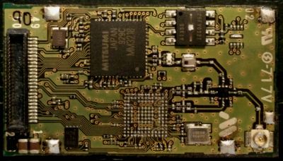
WiFi Module
Introduction
There appear to be 3 WiFi modules at use in the DSi. These implement both the "old" WiFi chip (MM3315/MM3218) for DS-mode backwards compatibility, as well as a new Atheros 6k-based WiFi chip. The DS WiFi is configured through profiles 1-3 and is limited to 802.11b 1-2Mbps and WEP encryption while the Atheros supports 802.11g rates and WPA encryption, configured through profiles 4-6.
Next to the WiFi chips, these modules also carry the NVRAM chip. The DSi only uses a tiny portion of the 128KB available for startup data, calibration, and user settings. Newer revisions of this board have a SPI EEPROM that has no backing memory for most of the 1Mbit address space (presumably as cost savings?). Thus, older modules can be used for installing the "dslink" WiFi loader (to be launched in DSi mode via save-game hacks in DSi hybrid games), while newer modules require a hardmod (chip replacement) to achieve this (as demonstrated by khmann, using an ST M34PE20 chip as replacement). All revisions of the module have footprints for both large and small NVRAM chip, and the change to the limited chip occurred prior to the release of the dslink exploit.
The Mitsumi WiFi is controlled through data in the NVRAM (eg: calibration data, allowed channels), while the Atheros configuration is stored in the other tiny IC on the board, an I2C EEPROM.
The pinout of the connector can be found in FCC documents (see below). This connector includes pins for JTAG access to the Xtensa core in the Atheros chip (using 3.3V signals, though the 1.8V rail needs to be supplied from an external source as well). It presumably uses the same debug interface as found in the ESP8266 and ESP32 chips (which also use Xtensa CPUs), though no reports of people attempting to connect to it have been found at the time of writing.
If this module is disconnected the DSi turns on to a black screen, because it can't read the NVRAM. If the DSi doesn't like the data contained on the module it will give either error 0000FEFE or 0000FE00 at poweron. See stage1 for more information.
Models
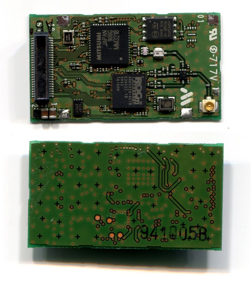
The original DSi DWM-W015 module features two wireless chips; a Mitsumi MM3218 for DS compatibility and a more modern Atheros AR6002G BGA which share the antenna through an RF switch. It also features 1Mbit of SPI EEPROM (ST M45PE10) for NVRAM. It has enough space to store a full copy of the old DS firmware.
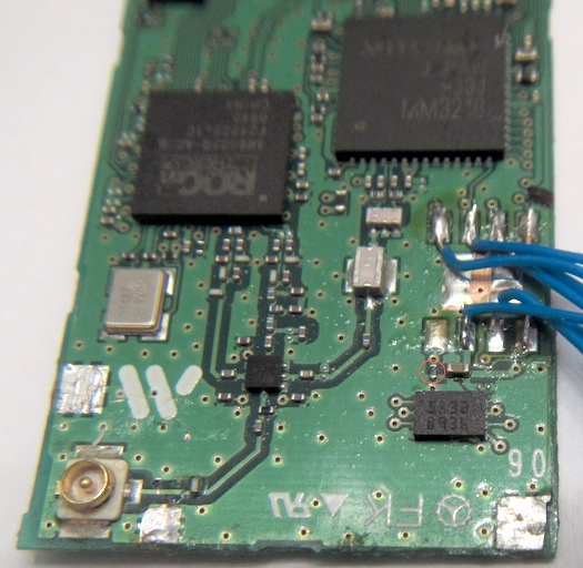
The updated DWM-W015A module uses a tiny "5A32" chip as NVRAM (UDFN/XSON, as opposed to the SOIC-sized chip in the older revision). Only the first and last few memory blocks are actually backed by a nonvolatile memory, other addresses return garbage.
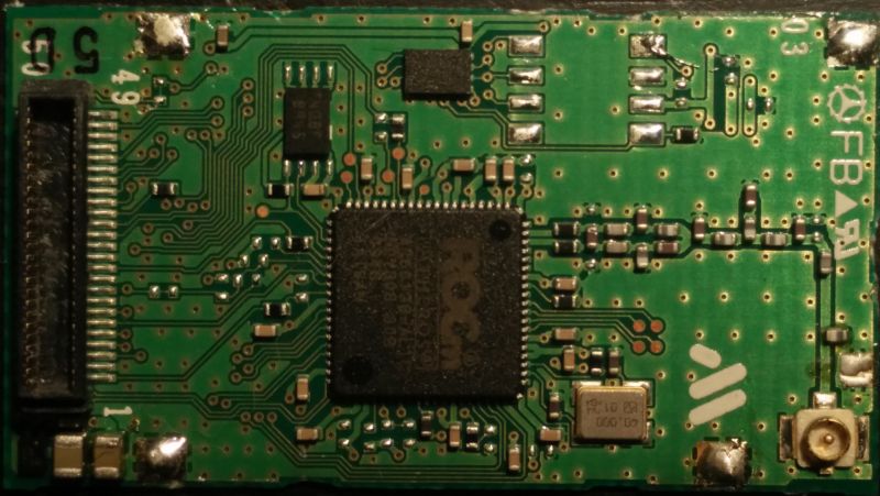
The DSiXL or DSi/LL module is labeled DWM-W024, and includes only an Atheros AR6013G-AL1C, a 5A32 variant, empty SPI flash pads, and another small chip, the Atheros-native I2C configuration. For reference, the 3DS DWM-W028 module is reported to use an Atheros AR6014G-AL1C. The connector pinout is unchanged. These AR601x chips contain the combined functionality of both the AR6002 and MM3218 chips found on the DWM-W015.
Photos
DWM-W015
DWM-W015A
Note the circle in this image shows a 10k resistor from pin 5 WP to GND, which the ST M45PE10 datasheet indicates will write-protect the first 64K. To disable this protection according to the SPI datasheet, remove the resistor and solder pin 5 to pin 6 VCC.
DWM-W024
Debugging the Ath6k Xtensa CPU
In case you want to run your own code on it (and subsequently need to debug it), the Atheros chip has two debug facilities: UART and JTAG. UART is a simple serial connection for printf-debugging, while JTAG can be used for single-stepping, breakpoints, etc.
NOTE THAT BOTH UART AND JTAG USE 1.8V LOGIC LEVELS. DO NOT DRIVE WITH 3.3 OR 5.0 V!!!
UART
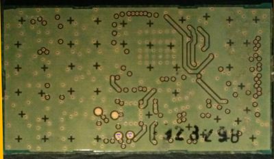
Serial communication on the Xtensa side can be done as described in GBATEK. On the DWM-W015, the UART testpoints appear on the bottom side of the PCB, near the edge (see below). On the DWM-W024, RX and TX are probably one of the four testpoints on the top side (see above).
JTAG
The four primary JTAG pins are exposed on the connector to the main board. However, the AR6002 has two extra pins that control JTAG functionality: JTAG_nRST and EJTAG_RST. They are marked in the image below, and they work as follows:
- JTAG_nRST resets the CPU core when pulled low. Some debuggers use this signal.
- EJTAG_RST is latched on chip powerup. If high, after a 'system' reset (read: the nWIFI_RST on the connector is pulled low), the Xtensa CPU is held at reset until JTAG_nRST is brought high. If EJTAG_RST is low, nothing special happens.
Thus, if your debugger has a JTAG_nRST signal (and you want to use it), pull EJTAG_RST to VDD18, and connect JTAG_nRST to your debugger. Otherwise, pull EJTAG_RST to ground (or leave it floating as-is, it probably has an internal pulldown).
As debugger, OpenOCD (or its fork for the ESP32) and any JTAG dongle compatible with it should work. Note that all JTAG communications use 1.8V! Using a higher voltage will kill the AR6002!
DWM-W024 testpoints
The DWM-W024 has four testpoints with currently-unknown functionality. These are probably UART TX, UART RX, JTAG_nRST, and EJTAG_RST. However, which testpoint is which signal is not yet known.
Documents and external links
- FCC "label location" document of the DWM-W015 (includes pinout)
- FCC "label location" document of the DWM-W024 (includes pinout)
- File:3002 Datasheet.pdf MM3315 aka RF3002 datasheet (old DS WiFi baseband chip)
- File:9008-pk020 Rev(B).pdf RF9008 datasheet (old DS WiFi RF chip)
- File:AR6002 Atheros.pdf.zip AR6002 datasheet (zipped to circumvent wiki upload size limits)
- GBATEK's information on the AR6002.
- MM3218 and AR60xx chip pinouts on GBATEK
