Difference between revisions of "Hardware"
Jump to navigation
Jump to search
(Moved the Test Points section to a page of its own, called, unsurprisingly, Test Points.) |
|||
| Line 38: | Line 38: | ||
[[Image:Nintendo-dsi-Glamor-Shot.jpg]] | [[Image:Nintendo-dsi-Glamor-Shot.jpg]] | ||
| − | |||
| − | |||
| − | |||
| − | |||
| − | |||
| − | |||
| − | |||
| − | |||
| − | |||
| − | |||
| − | |||
| − | |||
| − | |||
| − | |||
| − | |||
| − | |||
| − | |||
| − | |||
| − | |||
| − | |||
| − | |||
| − | |||
| − | |||
| − | |||
| − | |||
| − | |||
| − | |||
| − | |||
| − | |||
| − | |||
| − | |||
| − | |||
| − | |||
| − | |||
| − | |||
| − | |||
| − | |||
| − | |||
| − | |||
| − | |||
| − | |||
| − | |||
| − | |||
| − | |||
| − | |||
| − | |||
| − | |||
| − | |||
| − | |||
| − | |||
| − | |||
| − | |||
| − | |||
| − | |||
== References == | == References == | ||
Revision as of 21:48, 4 September 2009
| This article is a stub. You can help DSiBrew by expanding it. |
Specifications
- Includes (2) 0.3 Megapixel VGA Cameras
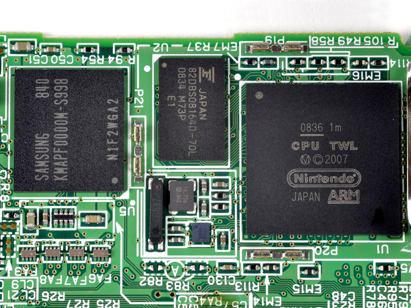
- 240MB(+16MB probably reserved for wear leveling purposes (e.g. replacing bad blocks)) Internal Flash Memory - Samsung kmapf0000m-S998 MOVI NAND - MMC Interface
- 16MB RAM - NEC uPD 46128512AF1 - DDR SRAM or a Fujitsu 128-Mbit FCRAM 82DBS08164D-70L
- (2) 256 x 192 3.25 Inch Displays, one of which has a resistive touch screen
- Backwards compatible with Nintendo DS games but not GBA games due to the lack of a gameboy cartridge port.
- Integrated ARM7/ARM9 cores clocked at 133mhz in real mode and downclocked to 66mhz for compatibility mode.
- PAIC3000D Sound Chip - possibly a TI codecs: AIC3 ????
- Mitsumi (MM3317A) or TI 72071B0 - Power supply and charger circuit ????
- SD/SDHC Card slot
- WiFi dongle with integrated 128KB SPI Flash for NVRAM, WiFi settings
Images
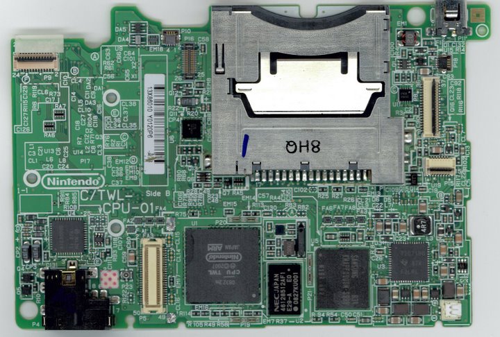
Front
The socket to the left of the ARM processor is the wifi chip socket.
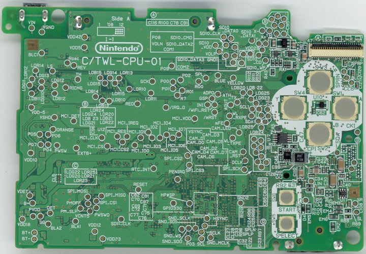
Back
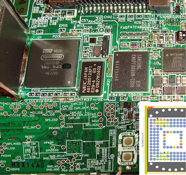
NAND pinout
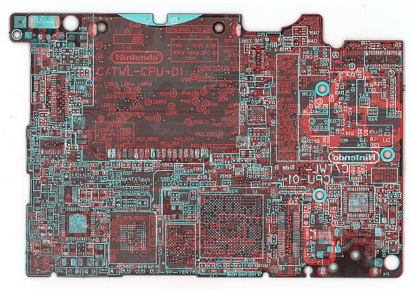
PCB overlay
CPU with new ram
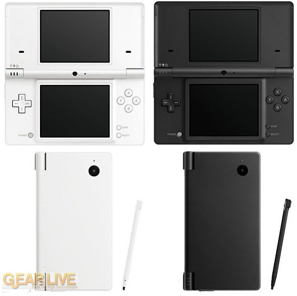
Glamor Shot
References
- http://en.wikipedia.org/wiki/Nintendo_DSi
- http://insidetronics.blogspot.com/2008/11/new-nintendo-dsi-teardown.html
- http://techon.nikkeibp.co.jp/english/NEWS_EN/20081111/161077/
- http://games.gearlive.com/playfeed/article/q408-nintendo-dsi-announced-larger-screens-dual-cameras-dsi-shop-store/
- http://www.ifixit.com/Guide/First-Look/Nintendo-DSi/714/1
